
GEMINI Dual-sided Displacement Inspection Device
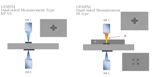
Observation / IR compatible
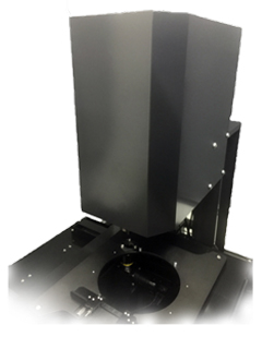
A fully automatic measurement device with unprecedented measurement precision
Resolution: 0.08μm/pixels (When using 20x)
Reproducibility: σ=0.5μm or under
Repeatability in the same spot: σ=0.05μm or under
Measurement Range: 6-8 inches *Other sizes possible
Equipped with Image AF and both upper and lower optics
Includes automatic optical axis adjustment function
Front to back exposure wafer misalignment and pattern shift
Micromachined hole deviation, etc.
Through-silicon pattern measurement via IR
MEMS devices, bonding deviation
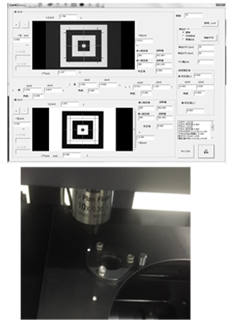
Automatic correction of top and bottom optics axis or angle misalignment
Detects correct values before measurements are taken based on the gauge fitted to the sample holder
This device cancels out differences in measurement values caused by drifts in time elapsed and temperature, etc.
| Measurement | front/back deviation, pattern centering, edge detection, simple length measurements |
|---|---|
| Functions | Automatic XY stage, automatic Z (up/down) driving Automatic alignment detection Measurement item and position recipe creation function Image AF and lighting control |
Specification
| Body | 1) Dedicated equipment stand (Can be changed depending on measurement sample size) 2) Z-axis: Z1, Z2±10mm drive, focus with Image AF 3) XY Automatic Stage Compatible with 6-inch and 8-inch wafer sizes (May also be compatible with other sizes) |
|---|---|
| Optics | 1) Optical instrument used for measurements: 1 replaceable objective lens 2) Objective lens: Choose from 5x, 10x, 20x, 50x, 100x (When using an IR model, the objective lens will be a special IR lens) 3) LED lighting: Visible observation - White 8W. IR Observation - 100WIR lighting |
| Camera |
1) CMOS Camera: 2 types for measurements, 1/2.3 inches, 1.67μm/pixel Measurement Resolution: When using a 10x objective lens - Approx. 0.04μm Imaging Range: Approx. 640μm×460μm |
| Measurements |
1)Front to back deviation measurement 2)Dimension measurement of pattern width, etc. 3)Simple on-screen length measurements 4)Image judgments via pattern matching |
| Measurement Reproducibility | σ=0.5μm or under |
| Repeatability in the same spot |
σ=0.05μm or under (Reproducibility fluctuates depending on the measurement sample. The above reproducibility is for a reference sample) |
| Measurement Uses | Wafer pattern linewidth measurements, bonded wafer misalignment, pattern shift Through-silicon pattern measurement via IR MEMS devices and micromachined hole deviation measurements |
IR Wafer Examination Device
We can detect defects and voids caused by bonding using IR observation.
Please inquire for more details.
KGM Gap Measurement Device
This device measures minute gap amounts in bonded wafers and devices.
Gaps of only a few μm can be detected using IR.
This device can also detect the measurement position and carry out all measurements automatically thanks to its automatic stage.
Please inquire for more details.
Bonding Equipment
We produce bonding equipment for each device based on customer requirements.
We can carry out bonding for silicon chips, glass substrates, and ceramic substrates. Bonding size and precision will be consulted upon as necessary.
Customization
We can make each kind of measurement device to order.
We will propose equipment based on what measurements are to be made and budget.
